
The Core Architecture: Beyond Transistors
Modern processors in 2025 are built on extreme ultraviolet (EUV) lithography at 2-nanometer and 1.4-nanometer nodes. A CPU is a complex integrated circuit containing billions of transistors—microscopic switches that toggle between on (1) and off (0) states. The fundamental building block is the CMOS (Complementary Metal-Oxide-Semiconductor) transistor, which uses a gate, source, and drain to control electron flow. When voltage applies to the gate, it creates a conductive channel, allowing current to pass. This binary operation underpins every calculation.
Processors in 2025 employ three-dimensional gate-all-around (GAA) FET architecture, replacing the older FinFET design. GAA wraps gates around all four sides of the channel, reducing leakage and improving drive current. This enables higher clock speeds—currently reaching 6.2 GHz in flagship desktop models—while maintaining thermal design powers (TDP) under 250 watts. Chiplet architecture dominates manufacturing: individual functional blocks (compute cores, cache, I/O, memory controllers) are fabricated on separate dies and interconnected via advanced packaging like EMIB (Embedded Multi-Die Interconnect Bridge) or UCIe (Universal Chiplet Interconnect Express). This approach yields higher yields and allows mixing different process nodes, such as high-density SRAM on 3nm alongside logic on 2nm.
Instruction Execution: The Fetch-Decode-Execute Cycle
Every operation begins with the fetch-decode-execute cycle. The processor uses a program counter (PC) to track the memory address of the next instruction. The fetch unit reads that instruction from the L1 instruction cache or main memory, then passes it to the decode unit. Decoders break complex instructions into simpler micro-operations (µops) that the execution units can handle. In 2025, ARM-based processors (Apple M4, Qualcomm Snapdragon X Elite) and x86 processors (Intel Core Ultra, AMD Ryzen 9000) both use macro-op fusion, merging multiple adjacent instructions into single µops to reduce decode bandwidth.
The decoded µops enter a reorder buffer (ROB). Out-of-order execution allows the processor to execute instructions as soon as their operands are ready, rather than in program order. For example, if instruction B depends on instruction A’s result, but instruction C is independent, C can execute before A finishes. The ROB tracks dependencies and commits results to architectural registers in the correct order. Simultaneously, branch prediction—using a combination of two-level adaptive predictors, neural network predictors, and tournament predictors—guesses the outcome of conditional jumps. Modern predictors achieve over 99% accuracy on typical workloads, but mispredictions incur a pipeline flush penalty of 15-30 cycles.
Caching Strategies: The Memory Hierarchy
Cache memory bridges the latency gap between the CPU core and main DRAM (DDR5 typically running at 6400-8000 MT/s in 2025). Each core contains a private L1 cache (split into 64KB instruction and 64KB data, with 1-cycle latency) and a unified L2 cache (512KB to 2MB, 5-10 cycle latency). L3 cache (16-128MB depending on chiplet count) is shared among cores on the same compute die, requiring 20-40 cycles. The replacement policy uses adaptive hybrid algorithms—often a blend of pseudo-LRU (Least Recently Used) and RRIP (Re-Reference Interval Prediction)—to balance temporal and spatial locality.
Hardware prefetchers aggressively predict data access patterns. Stream prefetchers detect sequential patterns; stride prefetchers identify constant offsets; and spatial memory streaming prefetchers capture multi-dimensional access patterns common in machine learning kernels. In 2025, many CPUs integrate on-chip HBM (High Bandwidth Memory) as an L4 cache, providing up to 2TB/s bandwidth with 100-cycle latency, especially in server and AI-focused SKUs. Instruction fetch and data load/store are decoupled via load/store queues and store buffers, allowing the execution pipeline to continue while memory requests complete.
Parallelism: SIMD, Vectors, and Multi-Threading
Single Instruction, Multiple Data (SIMD) units are critical for throughput. AVX-1024 (Advanced Vector Extensions) and SVE2 (Scalable Vector Extensions) now handle vector widths up to 2048 bits. Matrix engines—tensor processing units integrated into consumer CPUs—perform fused multiply-add operations on matrix tiles, accelerating AI inference and linear algebra by over 10x compared to scalar execution. These units use systolic arrays where data flows across multipliers in a rhythmic, pipe-lined fashion.
Simultaneous Multi-Threading (SMT), or Hyper-Threading on Intel, presents two logical cores per physical core by duplicating architectural state (registers, PC, buffers) while sharing execution resources. The scheduler interleaves threads to maximize utilization of idle execution ports. In 2025, AMD’s Zen 6 uses hardware-assisted thread scheduling that dynamically partitions ROB entries and cache ways per thread based on workload characteristics. Heterogeneous core designs are universal: performance cores (P-cores) optimized for high-frequency integer and floating-point workloads, and efficiency cores (E-cores) with shorter pipelines and lower voltage (0.55V vs. 0.9V) for background tasks. The OS scheduler and firmware (via Intel Thread Director or Arm’s DynamIQ) collaborate to place threads on optimal cores.
Power Management and Thermal Dynamics
Aggressive dynamic voltage and frequency scaling (DVFS) adjusts core clock speed based on current load. Per-core voltage regulators (VRs) on chip allow fine-grained control, transitioning between 200 states in microseconds. When a core is idle, it enters C-states: C1 halts the clock, C2 flushes caches and powers down the clock tree, and C6 cuts power entirely, saving register state in SRAM. The integrated power management controller (PMC) uses machine learning models trained on telemetry data to predict future load and pre-emptively scale voltage, reducing latency versus reactive governors.
Thermal density peaks at over 300 W/cm² in hot spots. Advanced cooling solutions include vapor chambers with integrated diamond-filled thermal interface material, single-phase immersion cooling in data centers, and microfluidic channels etched into the silicon substrate. Processors throttle (reduce frequency) if temperature exceeds 105°C, and emergency shutdown occurs at 120°C. Power gating isolates unused functional blocks, while clock gating prevents toggling of unused registers. In mobile and laptop SKUs, power allocation between P-cores and E-cores is dynamic, shifting up to 80% of the total budget to active cores.
Security and Virtualization Features
Hardware security extensions are mandatory in 2025. Trusted Execution Environments (TEEs) like Intel SGX2, AMD SEV-SNP, and Arm CCA create isolated enclaves where code and data are encrypted in memory and decrypted only inside the CPU. The memory encryption engine sits between the cache and memory controller, using AES-256-XTS encryption with per-enclave keys generated by an on-chip hardware random number generator. Side-channel attack mitigations include constant-time instructions for cryptographic operations, dynamic cache partitioning to prevent speculative access leakage, and serialization instructions (e.g., Intel’s LFENCE enhanced) that flush microarchitectural buffers.
Virtualization is hardware-accelerated via second-level address translation (SLAT), which maps guest virtual addresses to guest physical addresses to host physical addresses in a single hop. I/O memory management units (IOMMUs) enforce DMA remapping, preventing devices from accessing arbitrary memory. The hypervisor runs at a new privilege level (VMX root mode on x86, EL2 on Arm), and nested virtualization allows virtual machines to run their own hypervisors with minimal overhead. In 2025, the number of supported VM exits (transitions between guest and hypervisor) is halved compared to 2020 designs through microcode optimizations.
Interconnects and Memory Interfaces
The fabric connecting chiplets and to memory is as critical as compute. AMD’s Infinity Architecture 3.0 uses a mesh network with adaptive routing, achieving 2 TB/s bidirectional bandwidth between chiplets over 256-bit links. Intel’s EMIB bridges multiple dies with 4-8 TB/s throughput at extremely low latency (1-2ns). Chip-to-chip communication uses the UCIe standard, supporting 16 GT/s per lane with retimers that correct bit errors (RS-FEC, Reed-Solomon forward error correction). Inside the core, a ring bus (still used in smaller designs) or a 2D mesh connects execution units, L2 caches, and the memory controller.
Memory controllers support DDR5, LPDDR5X, and HBM3E. JEDEC standards in 2025 define DDR5-8000 as baseline, with on-die ECC correcting single-bit errors. Memory channels are increased: 4-channel on mainstream desktop (128-bit total width), 8-channel on workstations and 12-channel on server processors. The integrated memory controller uses a write-combining buffer to batch small writes into larger transactions over the 64-byte cache line bus. Near-memory compute capabilities allow simple atomic operations (fetch-and-add, compare-and-swap) to execute directly in the memory controller, reducing back-and-forth traffic.
The System Agent and Platform Integration
Every modern processor contains a system agent (also called uncore) managing I/O, security, and power. This includes PCIe 6.0 controllers (128 GT/s per lane) supporting direct GPU and NVMe connections, USB4/TBT5 controllers, and integrated Wi-Fi 7 and Bluetooth 5.4 MAC. The Display Engine drives up to eight 8K monitors at 240Hz via DisplayPort 2.1 and HDMI 2.2, using dedicated hardware encoders for AV1, HEVC, and VVC codecs at 8K 120fps. The Media Engine performs real-time video processing without touching the main cores.
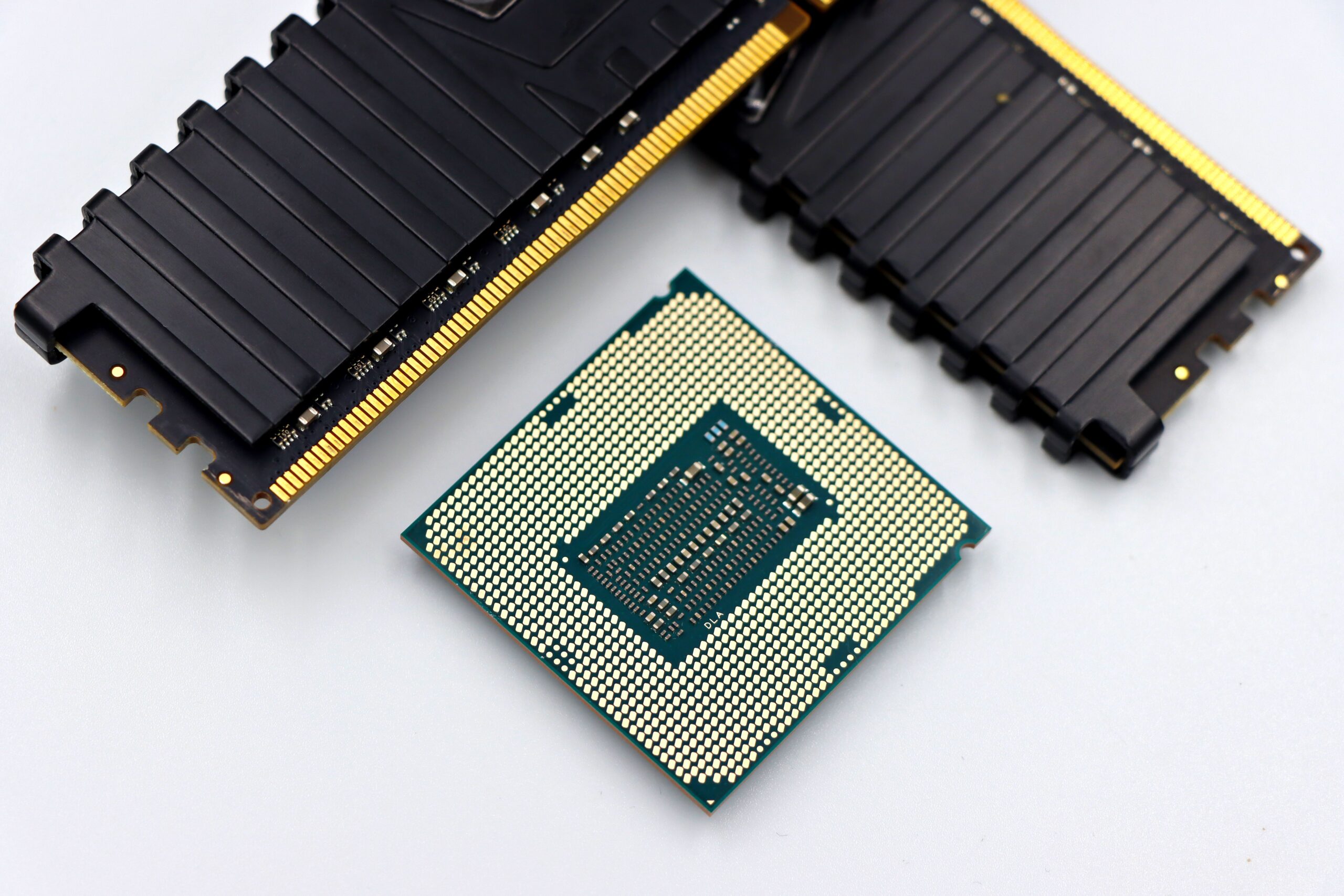
In 2025, all processors ship with a Neural Processing Unit (NPU) achieving 40-100 TOPS (INT8). The NPU features a data flow architecture with local SRAM and dedicated convolution, pooling, and activation units. It handles continuous on-device AI tasks: background blur in video calls, real-time language translation, audio source separation, and predictive text input. The NPU operates autonomously with its own DVFS domain, drawing under 1W for typical workloads. The processor packages all these components onto a single substrate with passive interposers that route signals across the 50x50mm package containing up to 1500 balls for land-grid array sockets.
Firmware and Initialization
On power-up, the processor executes microcode stored in on-chip ROM. This initializes voltage regulators, sets base clock frequencies, trains memory (running calibration sequences to determine timings and termination), and validates security boot keys (Root of Trust). The firmware (typically UEFI) then loads from SPI flash, configuring PCIe devices, ACPI tables, SMBIOS data, and power management policies. In 2025, platform firmware is modular (Firmware Volume blocks) with digital signatures enforced by the processor’s built-in authentication module. Secure boot chains verify every stage from microcode to OS loader; any tampering locks the system. After POST, the processor transitions to S0 active state and the scheduler begins dispatching workload threads across the full core cluster.